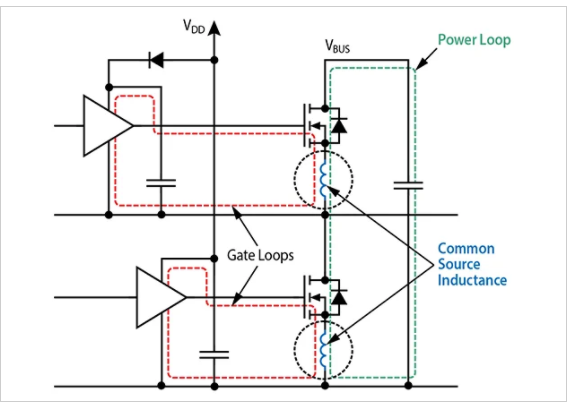
The use of GaN at higher frequencies than the aging power MOSFET is capable has put a spotlight on the degrading effects of parasitic inductance in a power conversion circuit [1]. This inductance hinders the extraction of the full benefit of GaN’s extra-fast switching capabilities with reduced EMI generation. For a half-bridge configuration, which is used in about 80% of power converters, the two main sources of parasitic inductance are; (1) the high-frequency power loop formed by the two power switching devices along with the high-frequency bus capacitor and, (2) the gate drive loop formed by the gate driver, power device, and high-frequency gate drive capacitor. The common source inductance (CSI) is defined by the part of the loop inductance that is common to both the gate loop and power loop.
Source : Layout Considerations for GaN Transistor Circuits – Technical Articles

